Table of Contents
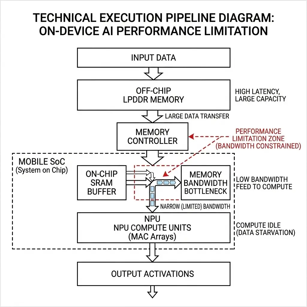
Why memory bandwidth limits on-device AI more than compute power becomes clear when examining how modern AI accelerators operate in real mobile systems. On-device AI performance is predominantly limited by memory bandwidth rather than raw compute capability. While modern NPUs boast high peak Tera Operations Per Second (TOPS), the energy and latency costs of moving vast amounts of model parameters and intermediate activations from slow, power-constrained off-chip LPDDR DRAM to fast on-chip compute units within mobile power limits create a severe data bottleneck. This results in compute units frequently stalling, leading to low sustained performance, poor power efficiency, and thermal challenges driven more by data movement than computation.
The semiconductor industry has achieved remarkable feats in scaling on-chip compute capabilities for AI workloads. Modern Neural Processing Units (NPUs) and accelerators within System-on-Chips (SoCs) routinely advertise tens of Tera Operations Per Second (TOPS), suggesting an abundance of processing power for on-device artificial intelligence for optimized operations. However, real-world performance often falls far short of these theoretical peaks. This discrepancy stems from a fundamental architectural imbalance: the rate at which data can be moved to and from these powerful compute engines – the memory bandwidth – has not kept pace with the exponential growth in computational throughput. This “memory wall” is the primary constraint limiting the scale, efficiency, and responsiveness of on-device AI for many workloads.
What Is Memory Bandwidth in On-Device AI Hardware
Memory Bandwidth refers to the maximum theoretical rate at which data can be transferred between the main memory (typically LPDDR DRAM in mobile SoCs) and the processing units (CPU, GPU, NPU). It is measured in Gigabytes per second (GB/s). This metric is critical because AI models, especially deep neural networks, are inherently data-intensive, requiring constant fetching of model weights, input data, and intermediate activations.
Compute Power, often expressed in Tera Operations Per Second (TOPS), quantifies the maximum number of arithmetic operations (e.g., Multiply-Accumulates, MACs) an accelerator can perform per second ideally. This figure represents the raw processing capability of the on-chip compute fabric, typically composed of large arrays of MAC units optimized for low-precision integer operations (e.g., INT8, INT4).
At the silicon level, compute power is relatively easy to scale by adding more MAC arrays, which are dense and power-efficient on-chip within a process node. Memory bandwidth, particularly to off-chip DRAM, is constrained by physical pin counts, I/O signaling speeds, and the power required to drive high-frequency data across PCB traces, given package and board constraints. This directly impacts the sustained performance of AI applications, as the device cannot continuously feed its compute units at peak rates. This hardware imbalance further illustrates why memory bandwidth limits on-device AI more than compute power in modern mobile AI accelerators.
How Memory Bandwidth Bottlenecks AI Inference
An AI inference operation involves a continuous flow of data for many models. Model weights and input data are initially stored in the main off-chip LPDDR DRAM. When a layer of the neural network is executed, these data blocks must be fetched from LPDDR, moved through memory controllers, potentially cached in on-chip SRAM buffers, and finally delivered to the NPU’s MAC arrays for computation. The results (intermediate activations) are then written back to SRAM and eventually to LPDDR, or passed to the next layer. This continuous data movement overhead is another reason why memory bandwidth limits on-device AI more than compute power in many real-world inference pipelines.
The critical bottleneck arises from the disparity in speed and energy cost:
- Data Movement Cost: Fetching a byte from off-chip LPDDR DRAM consumes orders of magnitude more energy (hundreds to thousands of picojoules per byte) than performing an 8-bit integer MAC operation on-chip (around 0.1 picojoules) in mobile SoCs. This makes data movement the dominant factor in overall power consumption for many AI workloads.
- Latency: Off-chip DRAM access latencies are typically in the hundreds of clock cycles. While data is being fetched, the high-TOPS compute units often sit idle, “stalled” and waiting for the necessary data to arrive.
- Arithmetic Intensity: Many AI layers, especially with small batch sizes (common in real-time on-device inference), have low arithmetic intensity – meaning few computations are performed per byte of data fetched for many neural network architectures. If a layer requires 1 FLOP per byte, a 50 GB/s memory bandwidth can only sustain 50 GFLOPs (0.05 TOPS), regardless of a 35 TOPS peak compute engine.
On-Device AI Architecture and Memory Bandwidth Constraints
On-device AI architectures are a deliberate, power-optimized compromise within mobile power/area budgets. SoCs typically feature a heterogeneous design, integrating a CPU, GPU, and a dedicated NPU or AI accelerator. All these components often share access to a unified external LPDDR DRAM.
The design philosophy prioritizes abundant on-chip compute (MAC arrays) because it’s significantly more power- and area-efficient to add these units than to proportionally scale external DRAM bandwidth beyond practical limits. Scaling external bandwidth requires more I/O pins, higher power I/O transceivers, and complex board routing, which are antithetical to mobile form factor and battery life constraints. This architectural choice implicitly pushes the burden of efficiency onto the software stack and model developers, relying on aggressive quantization, model compression, and sophisticated memory access scheduling to bridge the compute-memory gap. This is often supported by comprehensive development kits like the Qualcomm AI Engine SDK documentation.
While architectures like Apple’s “unified memory” reduce data copies and latency between CPU, GPU, and NPU by allowing direct access to a shared physical memory space, a hidden tradeoff is increased contention on the shared external LPDDR bus. If multiple high-demand AI tasks simultaneously saturate the shared LPDDR bandwidth, the benefit of “no copies” can be offset by increased arbitration overhead and effective latency for each component, depending on workload mix.
Performance Characteristics: Why Memory Bandwidth Limits On-Device AI
The memory bandwidth bottleneck manifests clearly when comparing theoretical peak performance against sustained real-world execution. On-device AI workloads frequently achieve only a fraction of the NPU’s peak theoretical TOPS in many real-world scenarios because the compute units are starved for data.
Quantization (e.g., INT8, INT4) is not merely a software optimization; it’s a fundamental architectural tradeoff baked into NPU design. Hardware is optimized to operate on reduced-precision data, directly reducing the volume of data movement and associated power consumption, at the cost of potential accuracy loss, which must be recovered during the training phase.
The following table illustrates the typical characteristics of different memory types and the performance impact of the memory bottleneck:
| Characteristic / Metric | On-chip SRAM (L1/L2/Scratchpad) | Off-chip LPDDR5X (Mobile) | HBM2e/3 (High-end Edge/Datacenter) |
|---|---|---|---|
| Typical Bandwidth | TB/s (e.g., 1-10 TB/s) | 50-100 GB/s | 500 GB/s to >1 TB/s |
| Typical Capacity | MBs (e.g., 1-100 MB) | GBs (e.g., 4-16 GB) | GBs (e.g., 8-64 GB) |
| Energy Cost (per byte fetch) | ~1-10 pJ/byte | 100-1000 pJ/byte | ~50-200 pJ/byte |
| Latency (typical) | ~1-10 ns (few cycles) | ~50-100 ns (100s of cycles) | ~20-50 ns (tens of cycles) |
| Performance Metric | Peak NPU Capability (e.g., Apple A17 Pro, Snapdragon 8 Gen 3) | Sustained On-Device AI Workload (Real-world) |
|---|---|---|
| TOPS (INT8) | 35-45 TOPS | 5-20% of Peak TOPS (e.g., 2-9 TOPS effective) |
| Compute Energy (per 8-bit MAC) | ~0.1 pJ | ~0.1 pJ |
| Memory Stall Cycles | Minimal (ideal conditions) | Significant (80-95% of compute idle) |
| Inference Latency | Low (e.g., <1ms for small models) | Higher due to memory stalls (e.g., 8ms of 10ms total) |
| Power Consumption | Dominated by compute (ideal) | Dominated by data movement (real-world) |
Real-World On-Device AI Workloads Affected by Memory Limits
The memory bandwidth bottleneck fundamentally dictates the feasible scale and complexity of on-device AI models. It forces model architects to prioritize highly optimized, memory-efficient models (e.g., high arithmetic intensity, aggressive quantization, efficient layer fusion) for deployment. This limits the types of advanced AI applications (e.g., very large language models, high-resolution multi-modal processing) that can run efficiently on current mobile platforms, pushing developers towards smaller, more specialized models or cloud offloading.
Furthermore, the constant “ping-pong” of data between on-chip buffers and off-chip DRAM, especially with batch size 1 inference, leads to unpredictable latency and potential “jitter” in real-time AI applications. The device’s responsiveness for AI tasks can feel inconsistent, as performance fluctuates based on whether the current layer’s data fits within on-chip memory or requires a costly off-chip fetch, directly impacting the perceived responsiveness and fluidity of the user experience.
Key Limitations of Memory Bandwidth in Mobile AI Accelerators
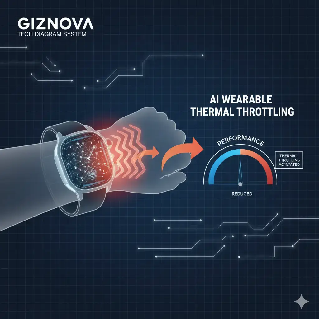
- Thermal Throttling from Data Movement: The energy cost of moving data, especially off-chip, significantly exceeds that of computation for many AI models. Under sustained AI workloads, a substantial portion of the device’s thermal output originates from the memory controllers and I/O transceivers, not just the compute units. This means thermal throttling limits are dictated as much by memory bandwidth utilization as by compute load, resulting in lower sustained performance and faster battery drain per effective operation.
- Constrained AI Application Scope: The memory bandwidth bottleneck forces a focus on highly optimized, memory-efficient models, limiting the deployment of larger, more complex AI models directly on-device within power and thermal envelopes.
- Diminishing Returns on Compute Scaling: The current architectural paradigm of “massive on-chip compute + external LPDDR” is rapidly approaching its fundamental limits for many AI workloads. Future generations of SoCs will see increasingly diminishing returns from simply adding more MAC units, as the memory wall will render them even more underutilized.
- Algorithmic Dependence for Viability: The continued viability of on-device AI with current hardware architectures is contingent upon sustained and aggressive algorithmic innovation in model compression, sparsity, and efficient network architectures for optimal performance. If future AI models become inherently less compressible, require higher precision, or demand larger working sets, the existing hardware paradigm will quickly become obsolete.
- System-Level Bandwidth Contention: Under sustained AI workloads, the operating system’s memory management unit (MMU) and scheduler, along with NPU drivers, constantly arbitrate access to the shared LPDDR bus depending on concurrent system activity. This introduces significant system-level overhead, latency, and potential thrashing, further reducing the effective bandwidth available to the AI workload below the theoretical maximum.
Why Memory Bandwidth Matters for Future On-Device AI Systems
The memory bandwidth bottleneck fundamentally dictates the ceiling for on-device AI capabilities on current mobile platforms. It’s a critical factor in determining battery life, sustained performance, and the complexity of AI models that can be deployed efficiently. This limitation is not merely an optimization challenge; it represents a core architectural constraint driven by silicon economics and power budgets.
To overcome this, a fundamental architectural redesign of the memory subsystem for future on-device AI is becoming necessary. Incremental LPDDR improvements are insufficient. Solutions may include the integration of compute much closer to or directly within memory (e.g., 3D-stacked compute-in-memory, specialized MRAM adjacent to NPUs, or heterogeneous memory hierarchies with small, ultra-high-bandwidth memory tiers). Such a paradigm shift will represent a significant increase in silicon complexity, cost, and potentially power, but it is critical to address the bandwidth ceiling and enable more capable on-device AI.
Key Takeaways: Memory Bandwidth vs Compute in Edge AI
For engineers designing edge AI hardware, understanding why memory bandwidth limits on-device AI more than compute power is critical for improving real-world inference efficiency.
- Memory Wall is Real: Despite high peak TOPS, on-device AI is predominantly memory-bound, not compute-bound, for many workloads.
- Data Movement Dominates: Fetching data from off-chip LPDDR is orders of magnitude more energy-intensive and slower than on-chip computation in typical mobile SoCs.
- Low Sustained Performance: Compute units are frequently idle, waiting for data, leading to a large gap between peak and sustained TOPS.
- Thermal and Power Implications: Data movement is a major contributor to thermal output and battery drain for many AI workloads.
- Architectural Compromise: Current designs prioritize power-efficient on-chip compute over costly off-chip bandwidth, relying on software optimizations to mitigate the gap within mobile power/area constraints.
- Future Architectural Direction: Overcoming this bottleneck may require a fundamental shift towards near-memory compute architectures, as incremental LPDDR improvements are insufficient.