Table of Contents
AI Image Processing ISP NPU architecture in modern System-on-Chips (SoCs) enables real-time, power-efficient computational photography directly on-device. The Image Signal Processor (ISP) handles high-throughput pre-processing tasks such as demosaicing, HDR merging, and noise reduction, while the Neural Processing Unit (NPU) accelerates deep learning inference for semantic segmentation, super-resolution, and computational bokeh. This tightly integrated silicon design minimizes latency, reduces memory bandwidth usage, and improves power efficiency within mobile thermal constraints.
AI’s evolution in consumer electronics has significantly shaped image and video processing. Traditional image pipelines, primarily handled by Image Signal Processors (ISPs), are now augmented by dedicated Neural Processing Units (NPUs) for complex AI model execution. This architectural shift addresses the computational intensity of deep learning models, which often exceed the capabilities of general-purpose processors or fixed-function ISPs for efficient inference, particularly as model sizes grow beyond tens of millions of parameters. This article details the engineering specifics of how these two critical SoC blocks collaborate to deliver advanced AI image processing capabilities, focusing on their architecture, performance, and silicon-level integration.
The 5 Essential Architecture Insights
AI Image Processing ISP NPU systems in modern SoCs are built around five essential architectural insights that define performance, efficiency, and real-time capability:
- Tight ISP–NPU integration within the SoC
- High-throughput image pre-processing in the ISP
- Dedicated neural inference acceleration in the NPU
- Optimized memory hierarchy and bandwidth management
- Sustained performance under thermal and power constraints
The following sections explore each of these architectural foundations in detail.
AI Image Processing Architecture in Modern SoCs
AI image processing within an SoC applies machine learning models, predominantly deep neural networks, to enhance, analyze, or manipulate image and video data. This is achieved through a specialized, synergistic architecture where the ISP performs initial, high-bandwidth, fixed-function image pipeline tasks, while the NPU accelerates computationally intensive AI model inference. This combined approach enables features from advanced noise reduction to real-time semantic segmentation. The synergy balances the ISP’s efficiency for structured, repetitive tasks with the NPU’s flexibility and computational density for adaptive, data-driven AI models, optimizing for both throughput and algorithmic complexity. This AI Image Processing ISP NPU model represents a fundamental shift in how heterogeneous compute blocks are coordinated within modern silicon architectures.
How AI Image Processing ISP NPU Works Inside a Modern SoC
The process begins with the camera sensor capturing raw image data, which is immediately fed into the ISP. The ISP executes a series of traditional image processing steps: demosaicing, noise reduction, HDR merging, color correction, and lens distortion correction. This pre-processed image stream, or derived feature maps, then passes directly to the NPU.
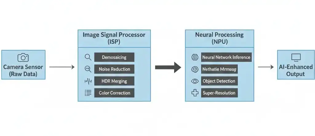
The NPU, optimized for parallel matrix operations, performs neural network inference to apply AI enhancements such as object detection, super-resolution, or computational bokeh. This direct data path between ISP and NPU minimizes latency and external memory bandwidth usage. Minimizing external memory traffic is crucial for power efficiency and avoiding performance bottlenecks. This is particularly true when processing high-resolution, high-frame-rate video streams, where the sheer volume of data can overwhelm shared system resources, often limited to tens of gigabytes per second on mobile SoCs.
ISP and NPU Microarchitecture Design
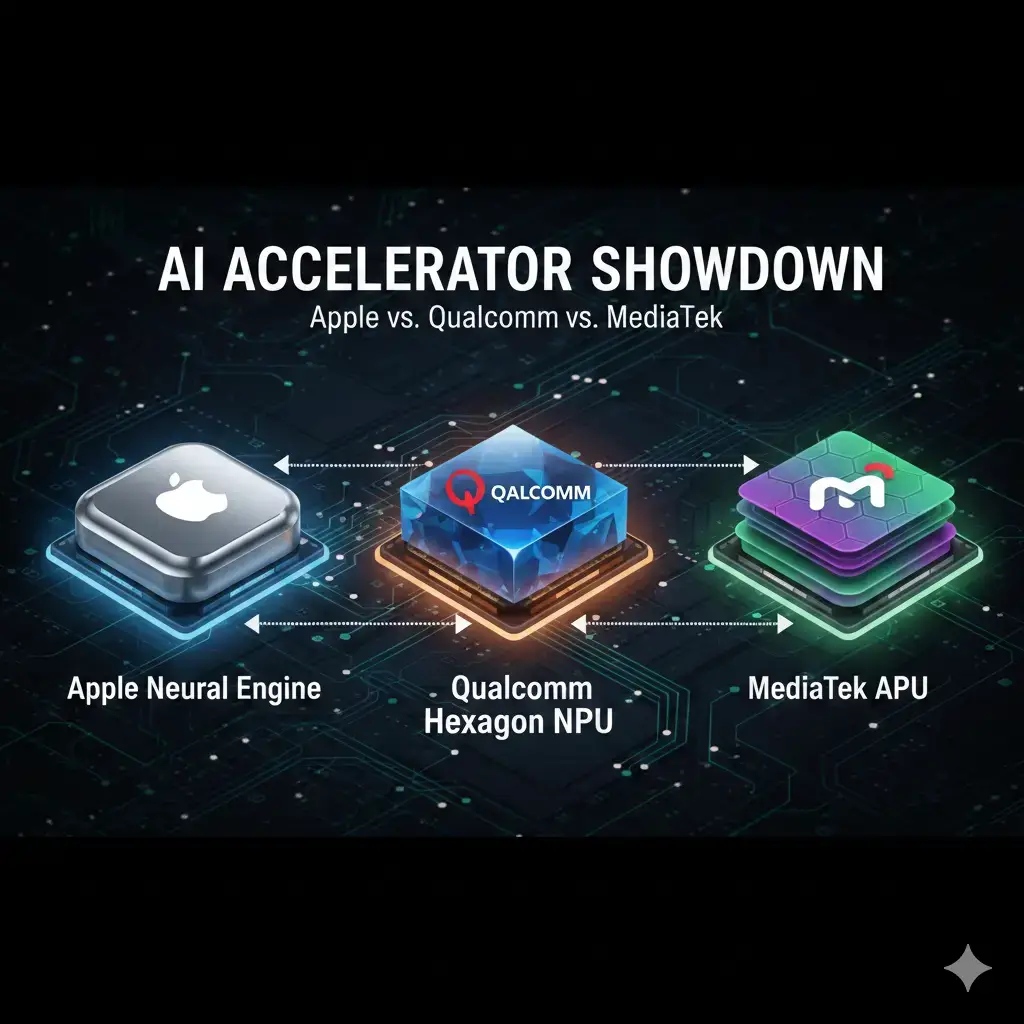
The ISP is a highly specialized, often fixed-function hardware block designed for parallel, real-time processing. It features dedicated high-bandwidth interfaces like MIPI-CSI to the camera sensor and utilizes internal scratchpad memory or DMA to system RAM (LPDDR5X) for intermediate buffers. ISPs from vendors examples include Apple’s Neural Engine, Qualcomm’s Hexagon NPU, and Google’s Tensor TPU architecture. These dedicated AI accelerators are deeply integrated within modern SoCs to optimize ISP and NPU collaboration. This tight integration allows for optimized power delivery and clocking schemes, which are vital for sustaining high throughput within stringent thermal and power envelopes, preventing performance degradation from thermal throttling during extended use.
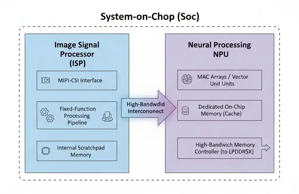
The NPU, or AI accelerator, typically comprises an array of specialized processing units (e.g., MAC units, vector units) optimized for neural network operations. It includes dedicated on-chip memory (scratchpad, caches) to reduce external memory accesses and connects to main system memory (LPDDR5X) via high-bandwidth controllers, typically accessing 8-16GB of RAM on high-end smartphones. The effectiveness of these on-chip memory structures is paramount for NPU performance. Frequent access to slower, higher-power external memory can severely limit achievable computational throughput and energy efficiency, particularly for large models or batch processing. This makes model size a critical factor for on-device deployment. Examples include Apple’s Neural Engine, Qualcomm’s Hexagon NPU, Google’s TPU, Intel’s AI Boost, and AMD’s XDNA NPU, all integrated at the same leading-edge process node as the CPU/GPU. High-bandwidth, low-latency interconnects are essential for efficient data transfer between the ISP and NPU.
Performance, Throughput, and Power Efficiency
ISPs are designed for high sustained throughput, handling real-time video streams such as 4K 60fps and 8K 30fps with consistent low latency. Their performance is measured by continuous processing capability rather than peak burst operations.
In contrast, NPUs are typically characterized using peak performance metrics such as TOPS (Tera Operations Per Second). However, sustained performance under thermal and power constraints provides a more realistic measure of real-world capability. Peak performance can only be maintained briefly before thermal throttling reduces clock speeds and power draw.
Key performance considerations in AI image processing ISP NPU systems include:
- Sustained throughput under mobile thermal limits
- Power efficiency measured in TOPS/Watt
- Memory bandwidth utilization and DRAM access patterns
- On-chip cache and scratchpad efficiency
- Synchronization overhead between ISP and NPU blocks
- Pipeline stall risks caused by processing imbalance
Overall system performance depends on seamless, low-latency coordination between the ISP and NPU. Any mismatch in processing rates can introduce bottlenecks, reduce effective throughput, and increase end-to-end latency in real-time imaging workloads.
Real-World Applications in Modern Devices
The ISP-NPU synergy powers numerous advanced imaging features in modern devices. Apple’s iPhone 15 Pro, with its A17 Pro chip, leverages the Photonic Engine (ISP + Neural Engine) for Smart HDR 5 and advanced Portrait mode depth mapping. Google Pixel 8’s Tensor G3 utilizes its custom ISP and TPU for features like Magic Eraser, Photo Unblur, and enhanced Night Sight. Samsung Galaxy S24 Ultra, with the Snapdragon 8 Gen 3, combines the Spectra ISP and Hexagon NPU for AI Zoom enhancements, Nightography improvements, and real-time semantic segmentation for generative image editing.
Architectural Constraints and Trade-Offs
Despite their capabilities, ISP and NPU architectures face inherent limitations. Power budgets and thermal dissipation constraints restrict sustained performance, especially in mobile form factors where total AI power may be limited to only a few watts.
On-chip memory capacity and external memory bandwidth are also critical bottlenecks. As AI models grow in parameter count and intermediate feature size, data movement between compute blocks and DRAM becomes increasingly expensive.
Key architectural trade-offs include:
- Model size versus real-time latency
- Precision reduction (quantization) versus accuracy
- On-chip memory size versus die area
- Performance scaling versus thermal headroom
- Portability across different NPU instruction sets
As AI Image Processing ISP NPU systems scale, engineers must carefully balance computational throughput, power efficiency, and memory hierarchy constraints to maintain real-time performance.
Why AI Image Processing ISP NPU Integration Matters
The AI Image Processing ISP NPU integration model represents a major shift toward heterogeneous computing in mobile silicon design. The tight integration of ISP and NPU is fundamental to modern computational photography and video processing. It enables on-device AI capabilities that enhance image quality, unlock novel user experiences, and provide privacy benefits by processing data locally. This local execution avoids the need to transmit sensitive user data to remote servers, mitigating privacy concerns and reducing reliance on network connectivity. This is a key advantage for edge devices, especially where network bandwidth is limited or inconsistent. This synergy is a key differentiator for SoC vendors and device manufacturers, driving innovation in areas like real-time video analysis, augmented reality, and generative image manipulation. It underscores the critical role of heterogeneous computing and specialized silicon design in advancing AI at the edge. For a broader comparison of edge processing models, see our guide on On-Device AI vs Cloud AI.
Key Takeaways
- ISP handles high-throughput, low-latency raw image pre-processing (demosaicing, HDR, noise reduction).
- NPU accelerates neural network inference for advanced AI image enhancements (segmentation, super-resolution).
- Tight integration within the SoC minimizes latency and power consumption for real-time AI.
- Architectures feature specialized hardware, dedicated memory, and high-bandwidth interconnects.
- Sustained performance and power efficiency (TOPS/Watt) are critical design metrics.
- This synergy enables advanced computational photography features in modern consumer devices.