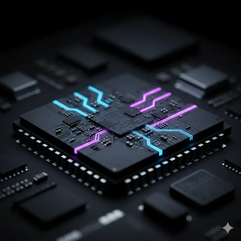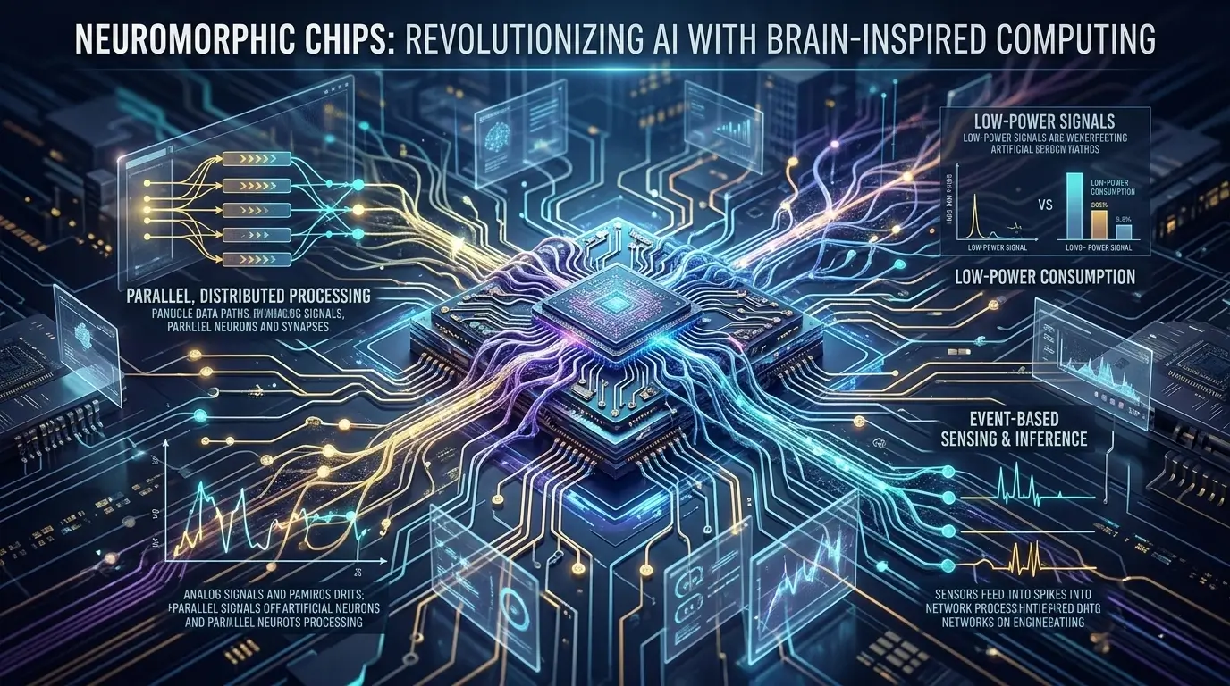
Neuromorphic chips are a class of brain-inspired processors designed for event-driven, asynchronous computation, fundamentally departing from traditional von Neumann architectures. They excel at processing sparse, real-time data streams with high power efficiency and low latency for specific workloads, making them ideal for always-on AI applications at the edge, particularly in power-constrained wearables. Their core innovation lies in co-locating compute and memory (in-memory computing) and activating logic only when a relevant spike event occurs, minimizing energy consumption from data movement and idle states.
The growing demand for ubiquitous artificial intelligence, especially in power-constrained edge devices like wearables, has pushed the limits of conventional computing architectures. While general-purpose CPUs and GPUs, along with specialized NPUs, have driven significant advancements in AI, their synchronous, clock-driven nature and inherent data movement overhead (the von Neumann bottleneck) present formidable challenges for always-on, low-power inference. This context has spurred the development of neuromorphic chips, a significant departure in silicon design that draws inspiration from the brain’s event-driven, massively parallel processing. For silicon architects, a clear understanding of Neuromorphic Chips Explained is crucial for designing the next generation of intelligent, energy-efficient systems.
Quick Summary
| Feature | Neuromorphic Chips |
|---|---|
| Computing Model | Event-Driven |
| Neural Model | Spiking Neural Networks (SNNs) |
| Power Efficiency | Extremely High |
| Latency | Ultra-Low |
| Best Use Cases | Edge AI, Wearables, Sensors |
| Main Advantage | Processes data only when events occur |
| Main Limitation | Limited support for modern foundation models |
| Bottom Line | Designed for highly efficient real-time AI workloads at the edge |
Table of Contents
What It Is
A neuromorphic chip is a hardware accelerator engineered to mimic the structure and function of biological neural networks, specifically Spiking Neural Networks (SNNs). Unlike traditional digital processors that execute instructions sequentially on data retrieved from separate memory, neuromorphic processors integrate compute and memory elements directly within “neuron cores.” These brain-inspired silicon devices operate asynchronously, meaning computation is triggered by discrete “spike” events rather than a global clock signal. This event-driven paradigm enables highly efficient processing of sparse data, in which only active neurons consume power, resulting in orders-of-magnitude lower energy consumption for specific AI workloads compared to conventional architectures.
How It Works
The operational principle of neuromorphic chips is rooted in event-driven computation. Instead of processing continuous data streams or large batches, these architectures react to discrete “spikes” – digital representations of neural impulses.
- Event-Driven Processing: When an input sensor (e.g., an event-based camera or microphone) detects a change or an event, it generates a spike. This spike is then transmitted to one or more neuron cores within the neuromorphic processor.
- Neuron Models: Each neuron core typically implements a programmable neuron model, such as an integrate-and-fire or leaky integrate-and-fire model. Upon receiving an input spike, the neuron’s internal state (membrane potential) accumulates. If this potential exceeds a predefined threshold, the neuron “fires,” generating an output spike.
- Synaptic Weights and In-Memory Computing: The connections between neurons are weighted, representing the strength of their influence. These synaptic weights are stored directly alongside the neuron processing units. This co-location, known as in-memory computing, is a critical design choice that bypasses the energy-intensive data movement between separate compute and memory blocks inherent in von Neumann architectures. When a spike arrives, the associated synaptic weight is applied, contributing to the receiving neuron’s membrane potential.
- Asynchronous Communication: Spikes propagate asynchronously across the chip’s communication fabric. There is no global clock dictating when operations occur; rather, each spike triggers subsequent computations locally. This can help reduce the power overhead associated with global clock distribution and allows inactive parts of the chip to consume near-zero dynamic power.
- Learning Rules: Many neuromorphic chips also incorporate on-chip learning engines, such as Spike-Timing-Dependent Plasticity (STDP). These engines allow the synaptic weights to adapt and learn from patterns in the spike timings, enabling continuous, unsupervised learning directly on the device.

This event-driven, asynchronous operation ensures that power consumption scales directly with the activity level of the network, achieving micro-watt standby and milliwatt active power for sparse workloads.
Architecture Overview
| Specification | Description |
|---|---|
| Architecture Type | Event-Driven SNN Processor |
| Compute Type | Dedicated NPU |
| Precision Support | INT8 / INT4 |
| Optimization Target | AI inference |
| Integration | SoC-level accelerator |
The architecture of a neuromorphic chip is fundamentally different from a traditional CPU or GPU. It is characterized by a highly parallel, distributed network of processing elements.
- Neuron Cores: At the heart of these specialized processors are thousands of independent neuron cores. Each core typically integrates a small number of programmable neurons, their associated synaptic memory, and local processing logic. This tight coupling of compute and memory is central to the in-memory computing paradigm, drastically reducing energy consumption from data transfers.
- Synaptic Memory: Within each neuron core, synaptic memory stores the weights that define the connections between neurons. This memory is often implemented using SRAM or emerging non-volatile memory technologies, optimized for low-power access during spike events.
- On-Chip Communication Fabric: An asynchronous, event-driven communication fabric (e.g., a Network-on-Chip, NoC) connects the neuron cores. This fabric is optimized for low-latency, sparse spike routing, ensuring that events propagate efficiently across the chip without the overhead of a global clock. The fabric’s design also dictates the maximum inter-core communication bandwidth, which can become a limiting factor for highly connected or dense SNNs.
- Event-to-Spike Converters: For interfacing with traditional frame-based sensors (e.g., standard cameras or microphones), dedicated event-to-spike converters are often integrated. These hardware blocks transform continuous or sampled sensor data into discrete spike streams that the neuromorphic architecture can process. However, the true efficiency of these brain-inspired silicon devices is realized when paired with native event-based sensors, which contrasts with the conventional approach of AI image processing using ISPs and NPUs for frame-based data.
- Learning Rule Engines: Many advanced neuromorphic processors include dedicated hardware for implementing on-chip learning rules, such as STDP. These engines enable the chip to adapt and learn from new data in real-time, without requiring off-chip training.
- Massive Parallelism: The architecture is characterized by massive parallelism, with thousands to millions of neurons and synapses operating concurrently. This design choice provides instantaneous, real-time responses to multiple concurrent events, crucial for low-latency applications in wearables.
This distributed, asynchronous design allows for significant power savings and real-time responsiveness by only activating the necessary computational elements when an event occurs.
Performance Characteristics
The performance of Neuromorphic Chips Explained is evaluated using metrics distinct from traditional FLOPs or TOPS, reflecting their unique operational model.
- Synaptic Operations Per Second (SOPs/s): This is the primary metric, quantifying the number of synaptic weight accumulations or updates performed per second. For instance, Intel’s Loihi 1 achieved up to 1.2 billion SOPs/s, while Loihi 2 scaled this to 8 billion SOPs/s per chip, demonstrating significant advancements in synaptic density and processing capability.
- Dynamic Power Scaling: A hallmark of these event-driven accelerators is their power consumption directly correlating with the actual spike activity within the network. Inactive neurons and synapses consume minimal power, leading to highly dynamic power profiles. For sparse SNN workloads, the average activity level is often less than 10% of peak, meaning the effective sustained power consumption is significantly lower than theoretical maximums. This enables micro-watt standby and milliwatt active power for continuous, sparse sensor processing. This dynamic scaling is critical for mobile power envelopes, where sustained power draw is typically limited to a few watts.
- Low Latency: Neuromorphic processors are designed for ultra-low latency inference. Event propagation between neuron cores on-chip typically occurs in microseconds (µs) per hop. For end-to-end tasks like keyword spotting or gesture recognition, latency can be in the low milliseconds (ms), providing immediate responses to input events without the fixed frame rates or batching delays inherent in synchronous systems.
- Energy Efficiency: The co-location of compute and memory, coupled with event-driven operation, results in exceptional energy efficiency per operation. BrainChip’s Akida 1000, for example, is quoted as achieving up to 1.2 TOPS/W for 8-bit operations, specifically for sparse event-based processing. This efficiency is critical for extending battery life in always-on wearable applications.
- Peak vs. Sustained Performance: While peak SOPs/s figures can be impressive, sustained performance for neuromorphic chips is highly dependent on the sparsity and rate of input events. Real-world applications often involve sparse data, meaning the average sustained compute and power draw are much lower than peak theoretical values, which is precisely where their efficiency advantage manifests.
Real-World Applications
The unique characteristics of neuromorphic chips make them particularly well-suited for a range of edge AI applications, especially in power-constrained and real-time environments like wearables.
- Always-On Keyword Spotting: For smartwatches and hearables, the ability to continuously listen for trigger words (“Hey Siri,” “Okay Google”) with minimal power consumption is paramount. Neuromorphic processors can process audio streams as sparse events, activating only when relevant acoustic patterns are detected, enabling multi-day battery life for such features.
- Gesture Recognition and Activity Monitoring: Wearable devices can use event-based vision sensors or IMUs (Inertial Measurement Units) to detect specific hand gestures or monitor physical activity. The low-latency, event-driven nature of neuromorphic silicon allows for instantaneous recognition and feedback, crucial for intuitive user interfaces and health monitoring.
- Bio-Signal Anomaly Detection: In medical wearables, continuous monitoring of physiological signals (e.g., ECG, EEG) for anomalies requires always-on processing. Neuromorphic chips can efficiently identify deviations from normal patterns in sparse bio-signal data, providing real-time alerts without draining the battery.
- Contextual Awareness: By integrating data from multiple sparse sensors (e.g., sound, motion, proximity), these brain-inspired silicon devices can build a real-time understanding of a user’s context, enabling more intelligent and proactive wearable experiences with minimal power overhead.
- Personalization and On-Device Learning: The integrated learning engines in some neuromorphic architectures allow for continuous adaptation and personalization. A wearable could learn a user’s specific speech patterns or gesture variations over time, improving accuracy and user experience without requiring data to be sent to the cloud for retraining.
These applications leverage the core strengths of neuromorphic chips: high power efficiency for sparse data, ultra-low latency, and the ability to perform continuous, real-time inference and adaptation at the very edge.
Limitations
Despite their promise, neuromorphic chips face several significant engineering challenges and inherent limitations that impact their widespread adoption.
- Debugging and Observability: The asynchronous, event-driven nature of these processors creates a profound debugging challenge. Spikes are transient, localized events, making it significantly harder to trace faults or understand complex network dynamics across thousands of asynchronous cores compared to synchronous systems. This necessitates specialized on-chip monitoring hardware and sophisticated software tools, adding silicon area and development complexity.
- Algorithmic and Software Ecosystem Immaturity: Unlike established deep learning frameworks with vast pre-trained models and standardized layers, Spiking Neural Networks (SNNs) require specialized algorithms, training methodologies, and a nascent software stack. Developers face a steep learning curve, limited off-the-shelf solutions, and a fragmented toolchain, increasing development cost and time-to-market. The “AI execution pipeline” for neuromorphic processors lacks the maturity of conventional AI frameworks, which is evident when comparing it to comprehensive toolkits like the Intel OpenVINO toolkit documentation that streamline AI inference deployment.
- Fixed Functionality vs. General Purpose AI: While configurable, the core architecture of neuromorphic chips is fundamentally optimized for SNNs and sparse, event-driven tasks. This implies a tradeoff: they are highly specialized accelerators, not general-purpose AI engines. They are inefficient or incapable of handling dense matrix multiplications or complex, non-spiking AI models prevalent in large language models or foundation models. This often necessitates a heterogeneous system design, adding complexity and potential communication bottlenecks with a host CPU or NPU, unlike the more versatile capabilities seen in conventional AI accelerators such as Snapdragon X Elite, Intel AI Boost, and AMD XDNA.
- Scalability for General AI and Foundation Models: The current neuromorphic paradigm, with its focus on sparse SNNs, faces significant limitations in scaling to the complexity of general AI or large multi-modal foundation models that rely heavily on dense operations and backpropagation. Future neuromorphic chips may remain specialized co-processors rather than universal AI accelerators.
- Ecosystem Fragmentation and Vendor Lock-in: The highly specialized hardware and nascent software ecosystem risk create significant fragmentation. Without dominant, open standards for SNN programming models, compilers, and hardware interfaces, developers may face vendor lock-in, stifling innovation and limiting mass-market adoption.
- Data Conversion Bottleneck for Legacy Sensors: The full benefits of neuromorphic chips are realized with native event-based sensors. However, the vast majority of existing sensors are frame-based. Converting this legacy data into efficient spike streams adds a pre-processing layer that consumes power, adds latency, and requires dedicated hardware, potentially negating some of the inherent efficiency advantages.
- Thermal Management for Transient Bursts: While average power is extremely low, peak activity (e.g., a burst of speech) can still generate localized heat spikes. Wearable thermal design must account for these transient, high-power events to prevent user discomfort or performance throttling.
- Battery Life Variability: Power consumption is directly proportional to spike activity. This means battery life will be highly variable depending on user behavior and environmental noise, potentially leading to inconsistent user experiences.
Addressing these limitations requires concerted efforts in hardware design, software development, and ecosystem standardization.
Why It Matters
Neuromorphic chips represent a critical evolutionary path for AI silicon, particularly for the pervasive deployment of intelligence at the extreme edge. Their significance stems from directly addressing fundamental engineering challenges that conventional architectures struggle with:
- High Power Efficiency: For “always-on” sensing and inference in battery-powered devices, the dynamic power scaling and near-zero idle power of neuromorphic processors are unparalleled. This enables multi-day to multi-week battery life for continuous AI tasks, fundamentally changing the design space for wearables and IoT.
- Ultra-Low Latency: The event-driven, asynchronous nature of these brain-inspired silicon devices allows for real-time responsiveness, crucial for safety-critical applications, intuitive user interfaces, and immediate feedback loops where sub-millisecond reaction times are paramount.
- On-Device Learning and Adaptation: The ability to perform continuous, low-power learning directly on the chip enables personalization and robustness to changing environments without relying on cloud connectivity, enhancing user experience and data privacy.
- Thermal Mitigation: By minimizing data movement and operating asynchronously, neuromorphic chips generate significantly less heat compared to traditional processors for equivalent sparse workloads. This reduces the need for bulky thermal dissipation solutions, enabling smaller form factors for compact devices.
- New Computational Paradigm: Neuromorphic chips offer a fundamentally different approach to computation, moving beyond the von Neumann bottleneck. This paradigm shift could unlock new classes of algorithms and applications that are inherently difficult or inefficient to implement on traditional hardware, paving the way for truly autonomous and adaptive edge AI.
As the demand for pervasive, intelligent, and energy-efficient computing continues to grow, neuromorphic chips are poised to play an increasingly vital role in shaping the future of AI hardware, especially where power, latency, and continuous operation are non-negotiable design constraints.
What are neuromorphic chips?
Neuromorphic chips are brain-inspired processors that use event-driven computation and spiking neural networks to perform highly efficient AI processing.
Why are neuromorphic chips more efficient?
They process information only when events occur and reduce data movement between memory and compute units.
Are neuromorphic chips used in consumer devices?
Today they are mainly used in research, edge AI systems, robotics, sensors, and specialized low-power applications.
Can neuromorphic chips run large language models?
Current neuromorphic architectures are optimized for event-driven AI workloads and are not well suited for large foundation models that rely on dense matrix operations.
Key Takeaways
- Neuromorphic chips are event-driven, asynchronous processors inspired by biological brains, designed for Spiking Neural Networks (SNNs).
- They achieve high power efficiency and ultra-low latency by co-locating compute and memory (in-memory computing) and activating logic only upon spike events, eliminating global clock overhead and minimizing data movement energy.
- Performance is measured in Synaptic Operations Per Second (SOPs/s), with power consumption dynamically scaling with network activity.
- Ideal for “always-on” edge AI in wearables, enabling tasks like keyword spotting, gesture recognition, and bio-signal anomaly detection with multi-day battery life.
- Significant engineering challenges remain, including debugging complexity, an immature software ecosystem, specialized functionality limiting general AI applications, and the need for event-based sensors to realize full efficiency.
- Despite limitations, neuromorphic processors offer a compelling solution to the power wall and latency demands of pervasive AI, representing a critical advancement in energy-efficient, real-time edge computing.