
Artificial intelligence is rapidly moving from cloud servers to smartphones, laptops, and edge devices. Features such as real-time transcription, AI image generation, local language models, and intelligent assistants increasingly rely on dedicated AI hardware inside modern chips. As a result, the shift from 5nm to 3nm semiconductor manufacturing has become one of the most important developments in AI hardware.
Many headlines suggest that 3nm chips are simply faster than 5nm chips. The reality is more nuanced. While 3nm technology improves transistor density and power efficiency, real-world AI performance also depends on memory bandwidth, NPU architecture, software optimization, and thermal management.
This guide explains the practical differences between 5nm and 3nm AI workloads, where users will notice improvements, and why process node size is only part of the story.
Quick Summary
- 3nm chips are not always dramatically faster than 5nm chips, but they are significantly more power efficient.
- The biggest advantage of 3nm technology is improved AI performance per watt, which helps devices run AI workloads longer without overheating.
- Modern 3nm AI chips can support larger NPUs, bigger caches, and more advanced on-device AI features.
- Memory bandwidth often matters more than TOPS numbers when running large language models and generative AI workloads.
- A well-optimized 5nm processor can still outperform a weaker 3nm design in certain AI tasks.
- For most users, the biggest benefits of 3nm are better battery life, lower temperatures, and more consistent AI performance.
For readers who want the short answer, the table below highlights where 3nm offers meaningful advantages over 5nm and where other factors matter more.
| Category | Winner |
|---|---|
| Power Efficiency | 3nm |
| Battery Life | 3nm |
| Sustained AI Performance | 3nm |
| Memory Bandwidth | Depends on Chip Design |
| NPU Performance | Depends on Architecture |
| Value for Existing Devices | 5nm Still Competitive |
| Future AI Workloads | 3nm |
Table of Contents
Why 3nm Doesn’t Automatically Mean Faster AI
A smaller manufacturing process does not guarantee better AI performance in every scenario. A well-designed 5nm chip with efficient software, strong memory bandwidth, and effective cooling can outperform a weaker 3nm implementation in specific workloads.
For AI tasks such as local LLM inference, image generation, speech recognition, and AI-enhanced photography, the quality of the NPU and memory subsystem often matters more than the process node itself. This is why some 4nm and 5nm chips continue to deliver excellent AI experiences despite newer 3nm alternatives entering the market.
The biggest benefit of 3nm is not raw speed. It is better performance per watt, allowing devices to run AI workloads longer while generating less heat.
What Changes When AI Chips Move From 5nm to 3nm?
According to publicly available industry guidance, 3nm technology can provide approximately 10–15% higher performance at the same power level or around 25–30% lower power consumption at the same speed. Logic density also increases significantly compared with 5nm.
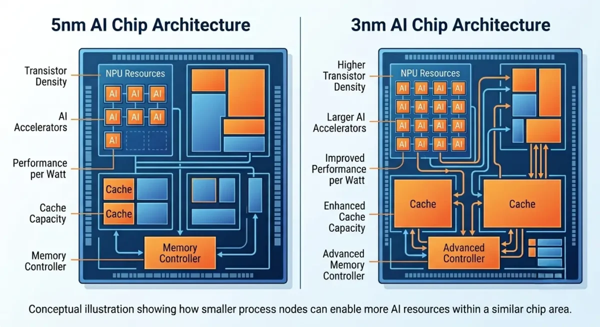
For AI processors, these gains create opportunities to integrate:
• Larger Neural Processing Units (NPUs)
• Bigger on-chip caches
• Additional AI accelerators
• Improved memory controllers
• Better thermal efficiency
According to TSMC’s 3nm process technology, these improvements allow chip designers to increase transistor density while improving power efficiency, making it easier to build more capable AI accelerators within the same silicon footprint.
Instead of dramatically increasing peak benchmark numbers, these improvements help devices sustain AI workloads more efficiently over longer periods.
5nm vs 3nm: Quick Comparison Table
Before diving deeper, here’s a simplified view of how modern 5nm and 3nm chips compare for AI processing.
| Feature | 5nm Process Node | 3nm Process Node |
|---|---|---|
| Transistor Density | High | Up to 1.8x Higher |
| Power Efficiency | Good | Up to 25–30% Better |
| Thermal Performance | Good | Better Sustained Performance |
| NPU Scaling | Advanced | Larger AI Accelerators |
| On-Chip Cache | Large | Larger and Faster |
| Battery Life | Good | Improved |
| Generative AI Support | Capable | Better Optimized |
| AI Performance per Watt | Strong | Superior |
The table highlights an important reality: the biggest advantage of 3nm isn’t necessarily peak AI speed. Instead, it is the ability to maintain AI performance while consuming less power and generating less heat.
For users running AI features throughout the day, efficiency often matters more than benchmark numbers.
Real-World Performance Differences in AI Workloads
Most AI applications do not operate in short bursts.
Tasks such as language model inference, image generation, speech recognition, AI-assisted editing, and real-time translation can keep a processor under load for several minutes at a time.
This is where the differences between 5nm and 3nm become easier to observe.
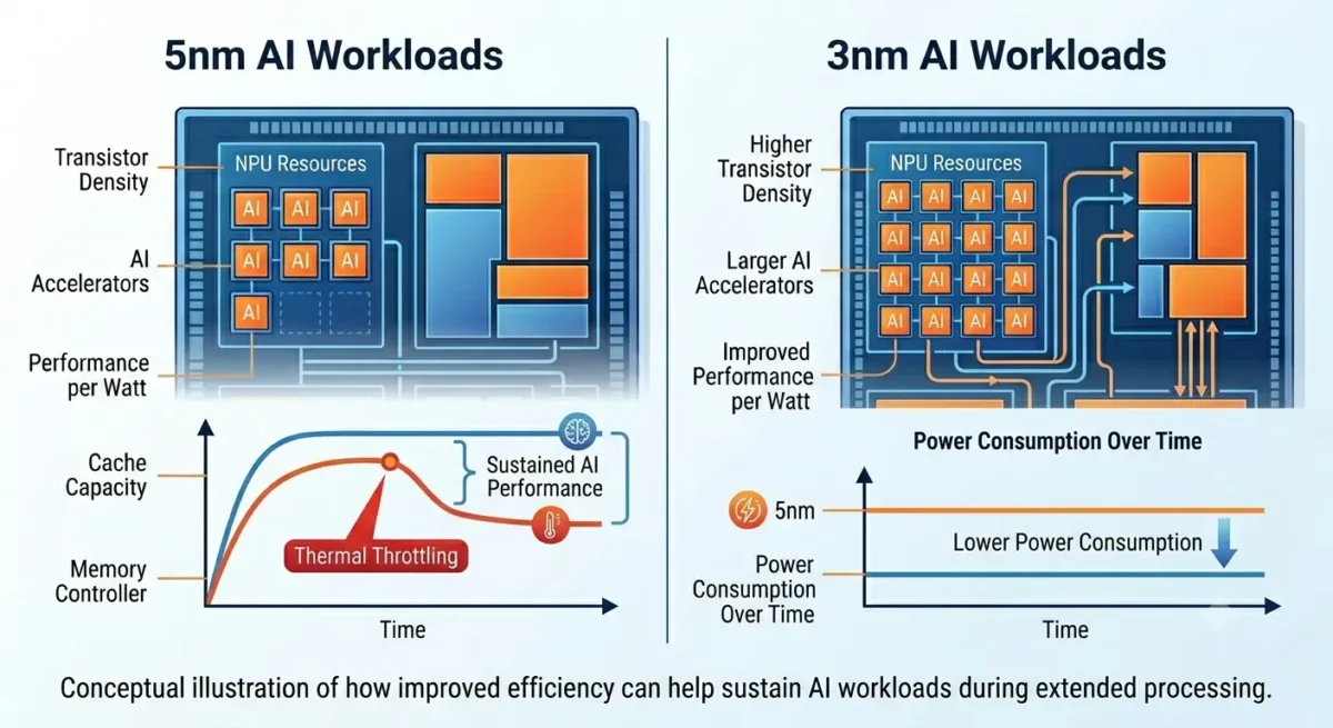
A modern 3nm chip generally requires less energy to perform the same workload. Lower power consumption means less heat buildup, allowing the processor to maintain higher clock speeds for longer periods.
For example, generating AI images locally or processing long voice recordings often creates sustained workloads. During these scenarios, a 3nm processor is more likely to maintain consistent performance without aggressive thermal throttling.
By comparison, a 5nm processor may initially deliver similar results but can reduce performance sooner as temperatures increase.
This doesn’t mean every 3nm chip automatically wins every benchmark. Architecture, cooling, and software optimization still play major roles.
However, when workloads become longer and more demanding, the efficiency advantage of 3nm becomes increasingly noticeable.
Peak AI benchmark numbers rarely tell the full story. As explored in our article Sustained AI Performance vs Peak TOPS: What Benchmarks Hide, long-running AI workloads often reveal performance differences that short benchmark tests fail to capture.
Why AI Power Efficiency Matters More Than Raw TOPS
Many chip manufacturers advertise AI performance using TOPS, or trillions of operations per second.
While TOPS numbers are useful, they rarely tell the full story.
A processor can achieve impressive peak TOPS ratings while still struggling during real-world AI tasks.
The reason is simple: AI workloads are rarely limited by compute power alone.
They also depend on:
- Memory bandwidth
- Cache capacity
- Software optimization
- Thermal behavior
- Data movement efficiency
This is why two chips with similar TOPS ratings can deliver very different user experiences.
For consumers, AI power efficiency is often the more meaningful metric.
An AI engine that performs slightly fewer operations while consuming significantly less power can provide a better overall experience by maintaining performance longer and extending battery life.
As AI features become more integrated into daily workflows, efficiency is becoming just as important as raw compute capability.
Real Device Examples
Apple A17 Pro (3nm)
Apple’s A17 Pro was among the first widely available 3nm smartphone processors.
The chip features a Neural Engine capable of delivering approximately 35 TOPS of AI performance while operating within the strict thermal limits of a smartphone.
What makes the A17 Pro important isn’t simply its TOPS rating.
Its improved efficiency enables more advanced on-device AI features, including image processing, voice recognition, and elements of Apple Intelligence.
The move to 3nm helps Apple deliver these capabilities without dramatically increasing battery consumption.
Apple M3 (3nm)
Apple’s M3 processor demonstrates how AI workloads benefit from more than transistor density alone.
The chip includes:
- 18 TOPS Neural Engine
- 100 GB/s memory bandwidth
- Unified memory architecture
The unified memory design allows the CPU, GPU, and Neural Engine to access the same data pool efficiently.
For AI workloads, this reduces unnecessary data movement and helps improve responsiveness.
The result is strong performance for tasks such as local language models, transcription, content creation, and AI-assisted productivity tools.
MediaTek Dimensity 9400 (3nm)
MediaTek’s Dimensity 9400 is designed with generative AI workloads in mind.
The chip offers roughly 50 TOPS of AI performance and supports high-speed LPDDR5X memory.
More importantly, MediaTek has focused heavily on improving on-device AI capabilities.
This includes support for larger language models, AI photography, and advanced voice assistants without relying entirely on cloud processing.
The efficiency gains provided by 3nm make these features more practical on battery-powered devices.
Samsung Exynos 2500 (3nm)
Samsung positions the Exynos 2500 as a major step forward for mobile AI.
The company claims approximately 59 TOPS of AI performance and a substantial improvement in NPU performance compared with the previous generation.
While independent testing will ultimately determine real-world performance, the chip illustrates how manufacturers are increasingly using additional transistor density to expand AI acceleration rather than simply boosting CPU speeds.
This reflects a broader industry trend toward AI-first chip design.
Snapdragon X Elite (4nm)
Snapdragon X Elite provides an important reminder that process node size is only one part of the equation.
Despite using a 4nm process, the chip delivers approximately 45 TOPS and supports memory bandwidth levels that enable strong AI PC performance.
The processor powers many Copilot+ PCs and demonstrates how architecture, software optimization, and memory design can compensate for differences in manufacturing technology.
For AI workloads, a well-balanced platform often matters more than the process node itself.
Memory Bandwidth: The Hidden Bottleneck in Modern AI
When discussing AI hardware, most attention is paid to TOPS numbers.
Many AI workloads are limited by memory bandwidth rather than compute performance. In fact, memory bandwidth often matters more than TOPS numbers, especially when running large language models and image-generation systems. We explore this concept in greater detail in our analysis of Why Memory Bandwidth Limits On-Device AI More Than Compute Power.
Think of memory bandwidth as the highway connecting storage and compute resources.
Even if the NPU is extremely powerful, it cannot process data efficiently if information arrives too slowly.
This becomes especially important for:
- Large Language Models (LLMs)
- Image generation models
- Multi-modal AI systems
- AI copilots
- Real-time assistants
A powerful AI accelerator can spend significant time waiting for data rather than performing computations.
In these situations, additional TOPS provide little benefit.
This is one reason why Apple’s M3, with its 100 GB/s memory bandwidth and unified memory architecture, performs so well in practical AI workloads.
Likewise, Qualcomm’s Snapdragon X Elite benefits from exceptionally high memory bandwidth that helps support local AI inference.
As AI models continue growing larger, memory bandwidth limitations will become even more important than raw compute power.
For many future workloads, memory architecture may determine the user experience more than transistor density alone.
Can Users Actually Notice the Difference Between 5nm and 3nm?
For most everyday tasks, the difference between a 5nm and 3nm chip is not immediately obvious.
Opening an AI assistant, applying a photo filter, or using voice dictation may feel similarly fast on both generations. Modern 5nm processors are already highly capable and can handle many AI-powered features without difficulty.
The gap becomes more noticeable during sustained AI workloads.
For example, users running local language models, generating AI images, editing videos with AI enhancements, or continuously using real-time transcription tools are more likely to benefit from 3nm technology.
In these situations, 3nm chips typically:
- Consume less power
- Generate less heat
- Maintain performance for longer periods
- Deliver better battery life
- Support larger AI models
The difference is similar to driving two cars with comparable top speeds. One vehicle may reach the same speed while consuming less fuel and staying cooler under heavy use. That’s essentially what 3nm technology brings to modern AI hardware.
For AI PCs, smartphones, and tablets, the biggest improvement isn’t necessarily speed. It’s consistency.
As AI workloads continue growing in complexity, sustained performance is becoming more valuable than short benchmark wins.
Limitations of 3nm Technology
Despite the advantages of 3nm manufacturing, it is not a magic solution for every AI challenge.
One common misconception is that moving to a smaller process node automatically solves performance bottlenecks. In reality, modern AI systems face several limitations that extend beyond transistor density.
The most significant limitations include:
Memory Capacity
Even the most advanced AI accelerator cannot efficiently run large models without sufficient memory.
Large language models require substantial RAM, and many consumer devices still face memory constraints regardless of the manufacturing process.
Memory Bandwidth
AI workloads constantly move data between memory and compute units.
When bandwidth becomes limited, the processor spends time waiting for information rather than performing useful computations.
This is one reason why memory architecture often has a greater impact on real-world AI performance than TOPS numbers alone.
Software Optimization
Hardware improvements only matter when software is optimized to use them.
Frameworks such as Core ML, TensorRT, ONNX Runtime, and Windows AI APIs play a major role in determining actual performance.
A poorly optimized application may fail to benefit from advanced hardware capabilities.
Thermal Constraints
Although 3nm chips are more efficient, they still generate heat.
Smartphones, tablets, and thin laptops have limited cooling capacity, which means thermal throttling remains a challenge during extended AI workloads.
Cost
Advanced manufacturing technologies are significantly more expensive.
This can increase development costs and affect device pricing, particularly in premium smartphone and laptop categories.
For these reasons, evaluating a chip solely based on its process node can be misleading.
The complete platform—including memory, software, cooling, and AI accelerator design—ultimately determines the user experience.
Which is better for AI Workload?
For most modern AI applications, 3nm technology offers a better overall foundation.
Its advantages include:
- Higher transistor density
- Better AI power efficiency
- Larger NPUs
- Improved battery life
- Better thermal behavior
- Stronger support for on-device AI
However, process node size should never be the only factor when comparing AI hardware.
A well-designed 5nm processor with strong memory bandwidth and optimized software can still outperform a weaker 3nm implementation in certain workloads.
This is particularly true for AI tasks that depend heavily on memory performance.
For buyers evaluating AI PCs, smartphones, or future edge AI devices, the smartest approach is to consider the complete platform rather than focusing exclusively on manufacturing technology.
The best AI experience comes from the combination of:
- Efficient NPUs
- High memory bandwidth
- Strong software optimization
- Effective thermal management
- Modern manufacturing processes
When all of these elements work together, users receive faster, more responsive, and more efficient AI experiences.
Is 3nm always faster than 5nm for AI workloads?
No. While 3nm generally improves efficiency and sustained performance, memory bandwidth, software optimization, and NPU architecture often have a greater impact on real-world AI performance.
Why does memory bandwidth matter for AI?
AI models constantly transfer large amounts of data between memory and processing units. Insufficient bandwidth can create bottlenecks that reduce overall performance, regardless of TOPS ratings.
Can a 5nm chip outperform a 3nm chip?
Yes. A well-designed 5nm processor with better architecture, memory performance, and software optimization can outperform a weaker 3nm implementation in certain AI tasks.
Is 3nm better for generative AI?
Generally, yes. The improved efficiency and higher transistor density of 3nm chips allow manufacturers to build larger NPUs and support more demanding generative AI workloads.
Does 3nm improve battery life?
Yes. One of the biggest benefits of 3nm technology is improved power efficiency, which can reduce battery drain during AI-intensive tasks.
Should I upgrade to a 3nm device for AI?
If you frequently use AI-powered features such as local language models, AI image generation, voice assistants, and content creation tools, a 3nm device can provide better efficiency and sustained performance. However, overall platform design remains just as important as the process node.
Key Takeaways
- Future AI devices will depend on a balance of efficient hardware, fast memory systems, and optimized software.
- 3nm technology improves AI performance primarily through better efficiency rather than dramatic speed increases.
- Lower power consumption helps devices maintain AI workloads longer without thermal throttling.
- Memory bandwidth often matters more than raw TOPS numbers.
- Larger NPUs and caches enable more advanced on-device AI capabilities.
- A strong 5nm design can still compete with a weaker 3nm implementation.
- Users are most likely to notice better battery life, lower temperatures, and more consistent AI performance.
Conclusion
The debate around 5nm vs 3nm AI workloads is not simply about which process node is smaller. While 3nm technology delivers meaningful improvements in efficiency, thermal performance, and AI scalability, real-world results depend on much more than transistor density alone.
Modern AI workloads increasingly rely on memory bandwidth, software optimization, and specialized AI accelerators. As a result, a balanced platform often matters more than peak benchmark numbers.
For most users, the biggest advantage of 3nm is not dramatically faster AI. It is the ability to run advanced AI workloads more efficiently, consume less power, generate less heat, and maintain performance for longer periods.
As on-device AI continues to evolve, the future will belong to chips that combine efficient manufacturing processes with intelligent architecture, powerful NPUs, and high-speed memory systems.